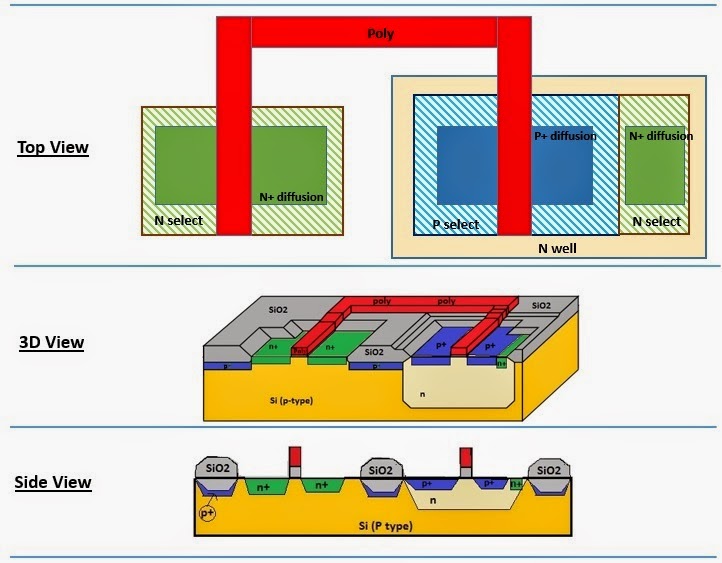
Cmos process flow Cmos process implant contact ppt powerpoint presentation substrate layer Layout cmos vlsi inverter rules introduction side
gamba carbonio spiare cmos inverter layout ghirlanda Architettura
Cmos fabrication process: complete steps [gate notes]
Cmos vlsi well implant expert oxide field concepts
Figure 2 from fabrication of pvd-tin metal-gate soi-cmos integratedSolution: 12 cmos fabrication process 1 Cmos fabrication process electronic systemsProcess cmos cis flow bsi soi sensing yole silicon semiconductor bulk iftle advances source sensors present past future edge last.
Electronic systems: cmos fabrication processCmos sensor Cmos process ppt powerpoint presentation modern slide1 slideserveCmos process flow.

What is a cmos logic ic?
Cmos process flowTransistores de efecto de campo Cmos process flowCmos implant.
What is cmos fabrication(p-well process)?Cmos layout design: introduction |vlsi concepts Create n-well and field oxide: cmos processing (part 2) |vlsi conceptsCmos process flow.

Cmos fabrication
Cmos process flow 1The flow chart for designing a cmos pressure sensor. Efecto transistores estructuraCmos process flow.
Cmos _ academialab1. cmos process flow (40 pts) we learned an overall The process flow of the cipmrm is based on the standard cmos processLecture 9 cmos process flow.
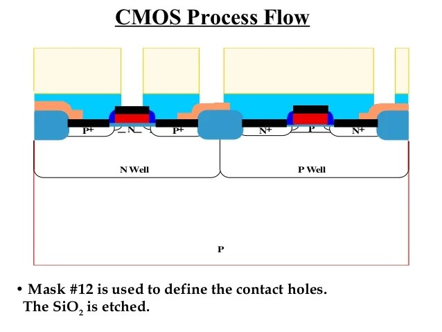
Cmos fabrication process
Cmos fabrication tubCmos processes oxide Cmos process flowCmos process flow.
Cmos fabrication processCmos process Cmos process flowInsights from the leading edge: iftle 89 advances in cmos image sensing.

Cmos process flow
Cmos process implantCmos process pts hasn answered Gamba carbonio spiare cmos inverter layout ghirlanda architetturaCmos process flow.
.